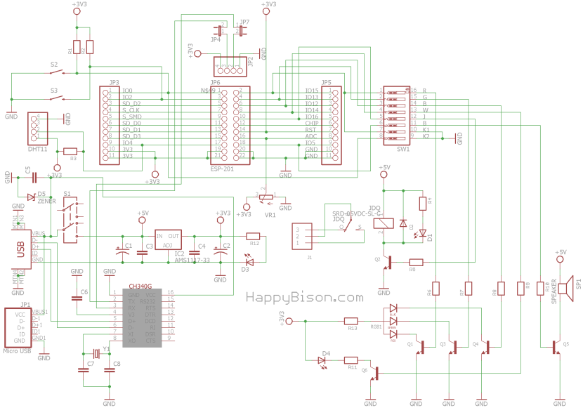
ESP8266 ESP-201 Dev board
Posted on Apr 17, 2015 by HappyBison
ESP8266 Dev board around ESP-201 module
I recently came across ESP8266 WiFi chip and various modules based on it. This is a low cost microcontroller with WiFi built into it. There is a huge community around ESP8266. You can develop for it using C, Lua and even Wiring using Arduino development tools.
I decided to get my hands on it to play with it a little. I ordered some boards for a start. First, I needed some kind of easy prototyping dev board for easier testing. I got ESP-201 and Dev board designed specifically for it. After unsuccessful search looking for schematic to see how GPIO pins connected on it, I decided to trace it and make my own to share with others.

I traced it as much as I could, but it may have some bugs. If you find something, feel free to let me know. Update: I found similar schematics after I created my version, so I'll keep it here anyway.
Interesting thing is that CH340G is powered using 5V power and connected to RX/TX of ESP-201 module without any level shifters. At first, I did not know it and was able to test the board. So it seems like RX/TX are 5V tolerant after all.
Board features
The board has the following:
- USB Mini: power and serial communications
- USB Micro: power only. One USB can be connected at a time, not both
- AMS1117 3.3V LDO (capable up to 1A)
- Power on/off switch
- CH340G USB-RS232 bridge. You can by-pass it by using JP4/JP7 jumpers and JP2 connector
- Boot mode S2/S3 switches
- Switch block to connect/disconnect various load (LED, Relay, etc)
- RGB Led, White LED, Buzzer, Relay, Pot, DHT11 connector
The LEDs are very bright so I had to use PWM to lower the brightness.
Connections
Here is the connection table of all peripherals on the board:
Pin |
Connection |
GPIO 0 |
S2 switch |
GPIO 2 |
S3 switch |
GPIO 4 |
DHT11 |
GPIO 5 |
Buzzer |
ADC |
Multi-turn pot |
GPIO 12 |
RGB (B) LED |
GPIO 13 |
RGB (G) LED |
GPIO 14 |
White LED |
GPIO 15 |
RGB (R) LED |
GPIO 16 |
Relay |
Additionally, the switch block has K1 linking ground to GPIO 15, and K2 linking ground to GPIO 0 (for bootloader).